- 您现在的位置:买卖IC网 > Sheet目录1219 > HC55185EVAL2 (Intersil)EVALUATION PLATFORM HC55185+T
�� �
�
�Application� Note� 9814�
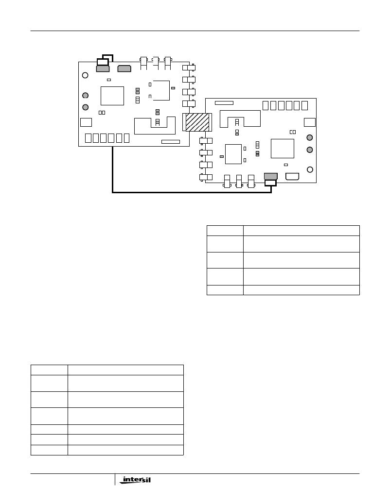
�Back� to� Back� Con?guration�
�MASTER�
�0�
�1�
�x�
�1�
�0�
�0�
�0�
�0�
�1�
�x�
�1�
�0�
�SLAVE�
�SECONDARY� POWER� CABLE�
�FIGURE� 15.� BACK� TO� BACK� CONNECTORS� AND� JUMPERS�
�Description�
�TABLE� 6.� SLAVE� BOARD� JUMPER� POSITIONS�
�The� back� to� back� con?guration� connects� two� evaluation�
�boards� together� at� the� PCM� interface.� The� PCM� output� data�
�from� one� board� is� the� PCM� input� data� to� the� other� board.�
�One� board� is� con?gured� as� a� master� for� clock� generation�
�and� the� other� is� con?gured� as� a� slave.� A� secondary� power�
�cable� provides� daisy� chain� power� to� the� second� evaluation�
�board.�
�Power� Supply� Connections�
�JUMPER�
�JP4�
�JP6�
�JP7�
�JP11�
�DESCRIPTION�
�Connects� the� receive� output� of� the� CODEC� (U6)� to�
�the� device� receive� input� VRX.�
�Connects� the� device� transmit� output� VTX� to� the�
�CODEC� amplifier� for� transhybrid� balance.�
�Connects� the� receive� output� of� CODEC� to�
�transhybrid� amplifier,� AC� coupled� by� C1.�
�Enables� the� on� board� logic� multiplexer.�
�Power� should� be� applied� to� the� evaluation� board� using� the�
�primary� power� cable.� Either� J5� or� J6� may� be� used.� Prior� to�
�applying� power,� the� voltage� setting� of� each� supply� should� be�
�veri?ed.� The� power� supplies� should� be� turned� off� while�
�mating� the� power� cables� to� the� evaluation� boards.�
�Jumper� Settings�
�.� All� jumper� settings� are� described� below.�
�TABLE� 5.� MASTER� BOARD� JUMPER� POSITIONS�
�In� this� con?guration� the� master� board� provides� the� clock� and�
�frame� sync� to� the� slave� board.� The� selection� of� the� clock� rate�
�is� arbitrary� and� may� be� any� of� the� available� frequencies.�
�The� ribbon� cable� used� to� connect� the� two� boards� at� J14� also�
�connects� the� ground� planes� of� the� two� evaluation� boards.�
�Having� returns� adjacent� to� the� high� speed� clock� edges� is�
�critical� to� reducing� board� level� noise.�
�If� transmission� quality� is� poor� verify� both� master� and� slave�
�JUMPER�
�JP4�
�JP6�
�JP7�
�DESCRIPTION�
�Connects� the� receive� output� of� the� CODEC� (U6)� to�
�the� device� receive� input� VRX.�
�Connects� the� device� transmit� output� VTX� to� the�
�CODEC� amplifier� for� transhybrid� balance.�
�Connects� the� receive� output� of� CODEC� to�
�boards� are� set� up� for� same� coding� scheme,� JP8.� In� addition,�
�verify� the� transhybrid� jumper,� JP7,� is� inserted� in� both� boards.�
�If� signal� quality� still� does� not� improve,� verify� JP12� of� the�
�slave� board� is� not� populated.�
�Analog� to� Analog� Veri?cation�
�The� back� to� back� con?guration� veri?es� the� complete� signal�
�transhybrid� amplifier,� AC� coupled� by� C1.�
�JP10,� POSN� 2� Sets� the� CODEC� master� clock� to� 512kHz.�
�path� of� two� evaluation� boards.� Full� duplex� transmission� is�
�provided� from� one� Tip� and� Ring� interface� to� the� other.� Both�
�JP11�
�JP12�
�Enables� the� on� board� logic� multiplexer.�
�Configures� board� as� master.�
�4-10�
�HC55185� devices� do� not� have� to� be� in� the� same�
�transmission� mode� (forward,� reverse� or� teletax)� for� proper�
�back� to� back� operation.�
�发布紧急采购,3分钟左右您将得到回复。
相关PDF资料
HE1015
BOOT CIRCUIT BREAKER 1POLE CLEAR
HE1020
BOOT CIRCUIT BREAKER 2POLE CLEAR
HE1050
BOOT CIRCUIT BREAKER 3POLE CLEAR
HE1070
BOOT CIRCUIT BREAKER 3POLE CLEAR
HFW30R-1STE1
HFW30R-1STE1-FFC/FPC CONN
HFW30S-2STE1
HFW30S-2STE1-USING HFW-P5SL
HHG
FUSEHOLDER AUTO INLINE FOR ATC
HHR
FUSEHOLDER 20A WATERPROOF ORANGE
相关代理商/技术参数
HC55185FCM
制造商:Rochester Electronics LLC 功能描述:75V RINGING SLIC WITH 53DB BAL FOR FXS - Bulk
HC55185FCMZ
功能描述:电信线路管理 IC 75V RINGING SLIC W/53DB BAL FOR FXS RoHS:否 制造商:STMicroelectronics 产品:PHY 接口类型:UART 电源电压-最大:18 V 电源电压-最小:8 V 电源电流:30 mA 最大工作温度:+ 85 C 最小工作温度:- 40 C 安装风格:SMD/SMT 封装 / 箱体:VFQFPN-48 封装:Tray
HC55185FCMZ96
功能描述:电信线路管理 IC 75V RINGING SLIC W/53DB BAL FOR FXS RoHS:否 制造商:STMicroelectronics 产品:PHY 接口类型:UART 电源电压-最大:18 V 电源电压-最小:8 V 电源电流:30 mA 最大工作温度:+ 85 C 最小工作温度:- 40 C 安装风格:SMD/SMT 封装 / 箱体:VFQFPN-48 封装:Tray
HC55185FCR
制造商:Rochester Electronics LLC 功能描述:- Bulk
HC55185FCRZ
功能描述:电信线路管理 IC SAME AS HC55185FCM EXCEPT MLF PKG RoHS:否 制造商:STMicroelectronics 产品:PHY 接口类型:UART 电源电压-最大:18 V 电源电压-最小:8 V 电源电流:30 mA 最大工作温度:+ 85 C 最小工作温度:- 40 C 安装风格:SMD/SMT 封装 / 箱体:VFQFPN-48 封装:Tray
HC55185FCRZ96
功能描述:电信线路管理 IC 32LD MFLP 75V W/53DB VAL FOR FXS RoHS:否 制造商:STMicroelectronics 产品:PHY 接口类型:UART 电源电压-最大:18 V 电源电压-最小:8 V 电源电流:30 mA 最大工作温度:+ 85 C 最小工作温度:- 40 C 安装风格:SMD/SMT 封装 / 箱体:VFQFPN-48 封装:Tray
HC55185GCM
制造商:Rochester Electronics LLC 功能描述:100V DB RINGING WITH GROUND START STATE - Bulk
HC55185GCMZ
功能描述:电信线路管理 IC 100V DB RINGING W/GROUND START STATE RoHS:否 制造商:STMicroelectronics 产品:PHY 接口类型:UART 电源电压-最大:18 V 电源电压-最小:8 V 电源电流:30 mA 最大工作温度:+ 85 C 最小工作温度:- 40 C 安装风格:SMD/SMT 封装 / 箱体:VFQFPN-48 封装:Tray